


Servicios Personalizados
Revista
Articulo
 Inglés (pdf)
 Artículo en XML
 Referencias del artículo
 Enviar artículo por email
Indicadores
-
 Citado por SciELO
 -
 Accesos
Links relacionados
-
 Similares en
SciELO
Similares en
SciELO
Compartir

 Permalink
Superficies y vacío
versión impresa ISSN 1665-3521
Superf. vacío vol.26 no.3 Ciudad de México sep. 2013
Characterization of nanostructured SnO2 films deposited by reactive DC-magnetron sputtering
Camacho-López M. A.1, Galeana-Camacho J. R.2, Esparza-García A.3, Sánchez-Pérez C.3, Julien C. M.4
1 Facultad de Química, Universidad Autónoma del Estado de México Paseo Colón y Tollocan, Toluca México, 50110, México.
2 Maestría en Ciencia de Materiales, Facultad de Química, Universidad Autónoma del Estado de México Paseo Colón y Tollocan, Toluca México, 50110, México.
3 Centro de Ciencias Aplicadas y Desarrollo Tecnológico, Universidad Nacional Autónoma de México, Circuito Exterior S/N, Ciudad Universitaria A.P. 70-186, C.P. 04510, México D.F. México
4 PECSA, Université Pierre et Marie Curie 4 place Jussieu, 75005 Paris, France.
Recibido: 20 de mayo de 2012
Aceptado: 19 de agosto de 2013.
Abstract
Nanostructured tin oxide thin films were deposited on silicon and glass slides substrates by reactive DC-Magnetron sputtering using a tin target in a mixture of argon and oxygen gases. The substrate temperature was varied in the range from 53 to 243 oC, keeping the other deposition parameters constant. The tin oxide films were characterized by: Scanning Electron Microscopy, Energy Dispersive Spectrometry, X Ray Diffraction, microRaman spectroscopy and UV-VIS spectroscopy. It was found that the substrate temperature has an effect mainly on the structural, morphological and optical properties of the thin films. At 53 and 90 oC the tetragonal crystalline phase was obtained while a mixture of crystalline phases (o-SnO2 and t-SnO2) was obtained at 148, 185 and 243 oC.
Keywords: DC-magnetron sputtering; Tin Oxide; Raman spectroscopy.
1. Introduction
Tetragonal SnO2 (cassiterite phase) in thin film form is a very attractive material due to its high transparency and good electrical conductivity. Additionally, these films are chemically inert, mechanically hard and can resist a high temperature making them attractive in a wide variety of potential technological applications, such as: window layer in solar cells, heat reflectors in solar cells, electrodes in opto-electronic devices[1], anode material for lithium ion batteries [2], fotocatalyst [3], among others. In particular, this material has been used in the sensing gas area taking advantage of the change in the conductivity properties of such material upon adsorption of the sensed gas [4,5].
Tin dioxide can exist in the orthorhombic-SnO2 (SnO2-II) phase too. This phase of tin oxide was synthesized at high pressure by Suito et al. in 1975 [6]. After that, the orthorhombic phase of SnO2 in thin film has been grown by Physical Vapor Deposition (PVD) and Chemical Vapor Deposition (CVD) methods. For instance, Lamelas et al. and Chen Zhiwel et al. have obtained the orthorhombic-SnO2 thin films by laser ablation [7, 8]. Applying thermal treatments in air to Sn films grown by RF-Sputtering, Sangaletti et al. reported a mixture of the tetragonal and orthorhombic phases of SnO2 for thin films [9]. L. Kong et al. have obtained the orthorhombic-SnO2 on Yttria Stabilized Zirconia (YSZ) substrate using the Metal Organic Chemical Vapor Deposition (MOCVD) technique [10]. To date, the orthorhombic phase of SnO2 has been obtained by using various synthesis methods [6-14], but to understand the experimental parameters that let to obtain the orthorhombic phase of SnO2, a lot of work is necessary in each synthesis technique. It is worth of mention that the properties of the orthorhombic SnO2 phase are, in general, very little-known.
Pure tetragonal SnO2, pure orthorhombic SnO2 or a mixture of these phases in its thin film form have been obtained by several deposition techniques including RF sputtering [15], reactive DC magnetron sputtering [16,17], pulsed laser deposition [7,8], among others. It is well known, that the properties of the deposited films strongly depend on the deposition parameters (atmosphere, substrate temperature, pressure, type of substrate) used during the film growth as well as on the deposition technique. The deposition parameters selection makes it possible to obtain thin films with a wide variety of features.
The aim of this work is to characterize the chemical, morphological, structural and optical properties of tin oxide films deposited on glass and silicon substrates by the reactive DC magnetron sputtering technique.
2. Experimental
SnO2 thin films were deposited using a non commercial sputtering system. The experiments were carried out with a base pressure of 1 x 10⁻³ mbar, using the constant current mode of a DC source (DC US GUN II Advanced Energy). To deposit the thin films a metallic tin disk from LESKER (99.9 % purity) was used as target and the sputtering process was done out using a mixture of argon and oxygen (Ar:O2 = 6:1) with a discharge power of 60 W. Silicon (100) wafers and glass slides were used as substrates keeping the target to substrate distance at 40 mm. The target was cleaned by a pre-sputtering for 5 min. The deposition time was set to 20 min. The substrate temperature was varied in the range from 53 to 243°C.
We used Scanning Electron Microscopy (SEM) to observe the surface morphology. Elemental analysis was performed using a microprobe coupled to a Philips XL30 scanning electron microscope.
X-ray diffractograms were obtained with a Siemens D-5000 diffractometer using the CuKa line (λ= 1.54 Â). The crystallite sizes, d, were calculated using the Scherrer's formula:  ; where λ is the X-ray wavelength employed, θ the diffraction angle of the (110) peak, and β is defined as the full width at half maximum (FWHM) after subtracting for the instrumental broadening.
Micro-Raman spectra were recorded at room temperature with the HR800-LABRAM system of Jobin-Yvon-Horiba using a 20 mW He-Ne laser (λ=632.8 nm) in the backscattering configuration. The UV-VIS transmission spectra were acquired using a Cary-5000 spectrophotometer of VARIAN. The Goodman's method was applied to calculate the refractive index and thickness of the deposited tin oxide films. Additionally, the film thickness was measured with a Dektak IIA profilometer. Finally, the band gap of the SnO2 films was calculated by the Tauc Method.
3. Results and Discussions
3.1 Energy Dispersive X-ray Spectroscopy and Scanning Electron Microscopy
The EDS measurements reveal only the existence of oxygen and tin in all the grown films. Figure 1 shows the atomic concentration of tin and oxygen in the as-deposited thin films as a function of the substrate temperature. The horizontal dashed lines (33.3 and 66.6 at. %) correspond to the SnO2 composition. It is observed that at 53 oC the deposited material has a composition corresponding to the tin dioxide. For substrate temperatures higher than 53 oC the oxygen content decreases as the substrate temperature increases, the O/Sn ratio changes from 2.0 (53 oC) to 1.7 (243 oC). This could be attributed to the preferential escape of the volatile element due to the higher mobility of the atoms as the temperature increases.
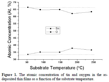
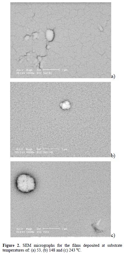
Figure 2 shows the surface morphology for a set of films deposited at a substrate temperature of 53 (a), 148 (b) and 243 oC (c). From the micrograph 2(a) one can see cracks running across the surface, which are generated due to the low temperature of the substrate. For higher temperatures, an homogeneous surface is obtained without cracks all longer.
3.2 X-ray diffraction
The X-ray diffraction patterns corresponding to the samples prepared at substrate temperatures of 53, 90, 148, 185 and 243 °C are shown in Figure 3. The peaks at 29 = 26.5°, 33.8°, 37.9°, 51.7° are the (110), (101), (200) and (211) reflection planes, respectively, which are characteristic of the cassiterite phase. It must be noted that as the substrate temperature increases up to 90 oC, the peaks associated to the cassiterite phase become sharper and more intense indicating that the crystallinity has clearly improved. On the other hand, at substrate temperatures higher than 90 °C, the presence of the (110) and (020) reflections, indicates the formation of the SnO2 orthorhombic phase (Figure 3c-e) [7,8].
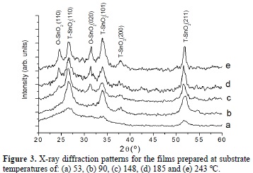
Figure 4a shows the crystallite size, calculated from the Scherrer's formula, as a function of the substrate temperature. It is clearly observed that the average crystallite size increases exponentially from 8 nm (at 153 oC) to 25 nm (at 243 oC) as the substrate temperature is increased.
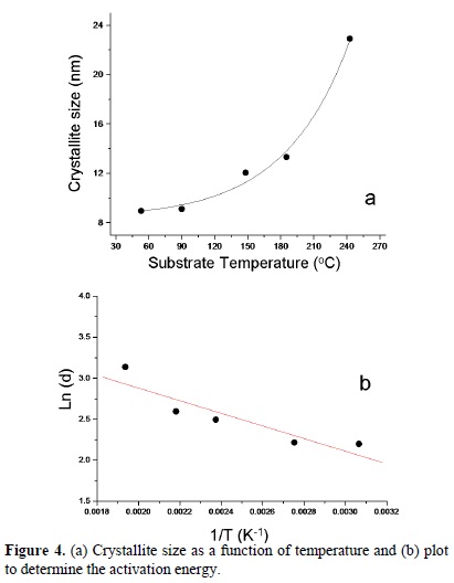
Assuming that the crystallite size follows a simple Arrhenius equation of the type:  where d0 is the initial crystallite size , Ea is the activation energy, T is the temperature, kB is the Boltzman's constant; it is possible to obtain the activation energy Ea from the ln(d) Vs 1/T plot (Figure 4b), using a lineal fitting of the experimental data the activation energy is approximately 20 kJ/mol.
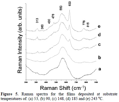
3.3 Micro-Raman spectroscopy
According to Beattie [18], SnO2 (casitterite phase) has a rutile structure with vibrational modes constituted by Raman active peaks at 123 (b1g), 476 (eg), 634 (a1g), 778 (b2g) and infrared active modes at 244 or 293 (eu), 477 (a2u) and 618 (eu) cm-1. In 1994, J. Zuo et al. reported that the Raman spectroscopy is a suitable technique to study size effects in SnO2 nanoparticles [19]. They showed that the Raman spectrum of nanosized SnO2 has two Raman bands centered at 358 (B1) and 572 cm-1 (B2) additionally to the vibrational modes of bulk SnO2. The band B2 corresponds to a surface mode and is very sensitive to the changes in crystallite size for nanosized SnO2. Studies on the size effects in SnO2 powders by Raman spectroscopy have been reported in references [19-22].
Micro-Raman spectra of the as-deposited thin films are shown in figure 5. The spectrum 5(a) corresponds to the film deposited at 53 °C. A wide band located at 570 cm-1 is the main feature in this spectrum corresponding to the surface mode of nanostructured cassiterite SnO2 [19,22]. Notice, there is a shoulder at 633 cm-1, attributed to the cassiterite phase, which is in good agreement with the XRD result. This result indicates that the deposited material at 53 oC consist of the nanostructured casiterite phase of SnO2. The spectrum 5(b) is for the film obtained at 90 oC. This spectrum exhibits peaks centered at 476, 633, and 773 cm-1 assigned to the SnO2 cassiterite phase [18]; a peak at 313 cm-1 appears in the spectrum and the main wide band shifts to lower frequencies (566 cm-1) indicating an increase in crystallite size. The Raman spectrum 5(c) corresponding to the film grown at 148 °C is constituted by peaks located at 476, 633 and 773 cm-1, which confirm that the material is grown adopting the rutile structure; the peak at 313 cm-1 is still present and the wide band is shifted to 559 cm-1. The spectra 5(d-e) correspond to the films grown at 185 and 243 oC. In the two spectra the peak at 634 cm-1 is the most intense and the wide band is shifted to 557 cm-1. These two facts indicate an increased crystallite size. Both results are in good agreement with the changes in the Raman spectra described by Zuo et al. when the crystallite size is increased in SnO2. Our results confirm that the wide band in the range 550-580 cm-1 is the fingerprint of the nanosized SnO2. It is worth mentioning that the peak located at 313 cm-1 is not commonly observed in the Raman spectrum of cassiterite SnO2. This peak was observed by S. H. Sun et al. for SnO2 nanobelts [23]. Further studies are necessary to understand the origin of the Raman peak located at 313 cm-1. To our knowledge, the Raman spectrum for SnO2 in its orthorhombic phase has not been reported yet.
3.4 UV-VIS spectroscopy
All the deposited thin films showed a high transmittance (85-90 %) in the visible region, absorbing in the UV region. As an example, in figure 6 the UV-VIS spectrum for the SnO2 thin film deposited at a substrate temperature of 243 oC is shown; there is an interference region in the spectrum. This feature makes it possible to apply the Goddman's model [24] for transparent films in order to calculate the thickness and the refractive index of the deposited materials.
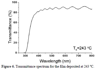
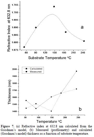
Figure 7a presents the results for the refractive index calculated at 632.8 nm as a function of the substrate temperature. The obtained results are in good agreement with the value reported in the literature (n=1.7) for tin oxide at 632.8 nm [15]. Figure 7b presents results on the thickness, determined using the Goddman's model; these results were compared to the results obtained from the profilometry measurements. It is pointed out that the thicknesses obtained by the two methods are different, with a maximum difference of 13 % which is considered reasonably. Notice that the results follow the same tendency in both cases.
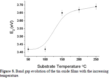
Using the transmittance spectra and the thickness, the band gap of the thin films for each substrate temperature was calculated. This was carried out following the Tauc method for crystalline solids [25]. Figure 8 presents the band gap as a function of substrate temperature; the band gap value increases from 3.42 to 3.69 eV, as the substrate temperature (or crystallite size) is increased. This result indicates that the band gap increases for the presence of the orthorhombic phase in the mixture of phases. Some researchers have reported that orthorhombic SnO2 phase has a wider band gap than that of the tetragonal phase. L. Kong et al. reported a value of 3.79 eV for the band gap of laser ablated orthorhombic SnO2 [10]. Chen Zhiwel reported 4.02 eV for orthorhombic SnO2 thin films obtained by laser ablation [8]. The band gap for tetragonal SnO2 in bulk is 3.6 eV at 300 K.
4. Conclusions
Nanostructured SnO2-x thin films were prepared by reactive DC-magnetron sputtering technique. It was possible to obtain the pure tetragonal phase (53 and 90 oC) or a mixture of tetragonal and orthorhombic phases (148, 185 and 243 oC) by varying the substrate temperature. Raman micro-spectroscopy confirmed the nanostructured nature of the SnO2. The films constituted by the mixture of phases were substoichiometric and presented a wider band gap than that of a pure tetragonal phase. The synthesis of pure orthorhombic SnO2 phase would be necessary to the aim to study its vibrational properties. To the best of our knowledge the Raman spectrum of orthorhombic phase has not yet been reported.
Acknowledgements
This work was supported by SIEA-UAEM under contract 3279/2012M. J. R. Galeana-Camacho thanks to SIEA-UAEM for the partial support received for the realization of this work.
References
[1] Matthias Batzill, Ulrike Diebold, Progress in Surface Science 79, 47 (2005). [ Links ]
[2] Min-Sik Park, Guo-Xiu Wang, Yong-Mook Kang, David Wexler, Shi-Xue Dou, Hua-Kun Liu, Angew. Chem. Int. Ed., 46, 750 (2007). [ Links ]
[3] D. Solís-Casados, E. Vigueras-Santiago, S. Hernández-López, M. A. Camacho-López, Ind. Eng. Chem. Res., 48, 1249 (2009). [ Links ]
[4] F. Hernandez-Ramirez, J. D. Prades, A. Tarancon, S. Barth, O. Casals, R Jiménez-Diaz, E. Pellicer, J. Rodriguez, M. A. Juli, A. Romano-Rodriguez, J. R. Morante, S. Mathur, A. Helwig, J. Spannhake and G. Mueller, Nanotechnology 18, 495501 (2007). [ Links ]
[5] X. Huang, J. Liu, Z. Pi, Z. Yu, Sensors 3, 361 (2003). [ Links ]
[6] K. Suito, N. Kawai, Y. Masuda, Mat. Res. Bull. 10, 677 (1975). [ Links ]
[7] F. J. Lamelas, S. A. Reid, Phys. Rev. B 60, 9347 (1999). [ Links ]
[8] Z. W. Chen, C. M. L. Wu, C. H. Shek, J. K. L.Lai, Z. Jiao, M. H. Wu, Critical Reviews in Solid State and Materials Sciencies 33, 197(2008). [ Links ]
[9] L. Sangaletti, L. E. Depero, A. Dieguez, G. Marca, J.R. Morante, A. Romano-Rodriguez, G. Sberveglieri, Sensors and Actuators B 44, 268 (1997). [ Links ]
[10] L. Kong, J. Ma, Z. Zhu, C.Luan, X. Yu, Q. Yu, Materials Letters 64, 1350 (2010). [ Links ]
[11] L. M. Cukrov, P. G. McCormick, K. Galatsis, W. Wlodarski, Sensors and Actuators B 77, 491 (2001). [ Links ]
[12] M. K. Kennedy, F. E. Kruis, H. Fissan, H. Nienhaus, A. Lorke, T.H. Metzger, Sensors and Actuators B 108, 62 (2005). [ Links ]
[13] Jordi Arbiol, Elisabetta Comini, Guido Faglia, Giorgio Sberveglieri, Joan Ramon Morante, Journal of Crystal Growth 310, 253 (2008). [ Links ]
[14] Marcelo Ornaghi Orlandi, Antonio José Ramirez, Edson Roberto Leite, and Elson Longo, Crystal Growth & Design 8, 1067 (2008). [ Links ]
[15] S. Hamzaoui, M. Adnane, Applied Energy 65, 19 (2000). [ Links ]
[16] M. Ruske, G. Bauer, J. Pistner, U. Pfafflin, J. Szczyrbowski, Thin Solid Films 351, 146 (1999). [ Links ]
[17] A. Martel. F. Caballero-Briones, R. Castro-Rodriguez, P. Bartolo-Pérez. Superficies y Vacío 17, 1 (2004). [ Links ]
[18] I. R. Beattie and T.R. Gilson, J. Chem. Soc. A., Phys. Theor. 2322 (1969). [ Links ]
[19] J. Zuo, C. Xu, X. Liu, C. Wang, C. Wang, Y. Hu, Y. Qian, J. Appl. Phys. 75, 1835(1994). [ Links ]
[20] A. Diéguez, A. Romano-Rodríguez, J. R. Morante, U.Weimar, M. Schweizer-Berberich, W. Gopel, Sensors and actuators B 31, 1 (1996). [ Links ]
[21] L. Albello, B. Bochu, A. Gaskov, S. Koudryavtseva, G. Lucazeau, M. Roumyantseva J. of Solid State Chemistry 135, 78 (1998). [ Links ]
[22] A. Diéguez, A. Romano-Rodríguez, A. Vilà, J. R. Morante, J. Applied Physics 90, 95 (2001). [ Links ]
[23] S. H. Sun, G. W. Meng, G. X. Zhang, T. Gao, B. Y. Geng, L. D. Zhang, J. Zuo, Chemical Physics Letters 376, 103 (2003). [ Links ]
[24] A. M. Goodman, Applied Optics 17, 2779 (1978). [ Links ]
[25] J. Tauc, Optical Properties of Solids, North-Holland, Amterdam, 1972. [ Links ]

